1. Reading Comprehension(每小题2分,共60分) (1) Device Technology Challenges Difficult challenges gating development of beyond-CMOS devices include those related to memory technologies, information processing or logic devices, and heterogeneous integration of multi-functional components, a.k.a. More-than-Moore (MtM) or Functional Diversification. One challenge is the need of a new memory technology that combines the best features of current memories in a fabrication technology compatible with CMOS process flow and that can be scaled beyond the present limits of SRAM and FLASH. This would provide a memory device fabrication technology required for both stand-alone and embedded memory applications. The ability of an MPU to execute programs is limited by interaction between the processor and the memory, and scaling does not automatically solve this problem. The current evolutionary solution is to increase MPU cache memory, thereby increasing the floor space that SRAM occupies on an MPU chip. This trend eventually leads to a decrease of the net information throughput. In addition to auxiliary circuitry to maintain stored data, volatility of semiconductor memory requires external storage media with slow access (e.g., magnetic hard drives, optical CD, etc.). Therefore, development of electrically accessible non-volatile memory with high speed and high density would initiate a revolution in computer architecture. This development would provide a significant increase in information throughput beyond the traditional benefits of scaling when fully realized for nanoscale CMOS devices. A related challenge is to sustain scaling of CMOS logic technology. One approach to continuing performance gains as CMOS scaling matures in the next decade is to replace the strained silicon MOSFET channel (and the source/drain) with an alternate material offering a higher potential quasi-ballistic-carrier velocity and higher mobility than strained silicon. Candidate materials include strained Ge, SiGe, a variety of III-V compound semiconductors, and carbon materials. Introduction of non-silicon materials into the channel and source/drain regions of an otherwise silicon MOSFET (i.e., onto a silicon substrate) is fraught with several very difficult challenges. These challenges include heterogeneous fabrication of high-quality (i.e., defect free) channel and source/drain materials on non-lattice matched silicon, minimization of band-to-band tunneling in narrow bandgap channel materials, elimination of Fermi level pinning in the channel/gate dielectric interface, and fabrication of high-κ gate dielectrics on the passivated channel materials. Additional challenges are to sustain the required reduction in leakage currents and power dissipation in these ultimately scaled CMOS gates and to introduce these new materials into the MOSFET while simultaneously minimizing the increasing variations in critical dimensions and statistical fluctuations in the channel (source/drain) doping concentrations. The industry is now addressing the increasing importance of a new trend of functional diversification, where added value to devices is provided by incorporating functionalities that do not necessarily scale according to “Moore's Law”. A longer-term challenge is invention and reduction to practice of a manufacturable information processing technology addressing “beyond CMOS” applications. For example, emerging research devices might be used to realize special purpose processor cores that could be integrated with multiple CMOS CPU cores to obtain performance advantages. These new special purpose cores may provide a particular system function much more efficiently than a digital CMOS block, or they may offer a uniquely new function not available in a CMOS-based approach. Solutions to this challenge beyond the end of CMOS scaling may also lead to new opportunities for such an emerging research device technology to eventually replace the CMOS gate as a new information processing primitive element. A new information processing technology must also be compatible with a system architecture that can fully utilize the new device. A non-binary data representation and non-Boolean logic may be required to employ a new device for information processing. These requirements will drive the need for new system architectures. The requirements and opportunities correlating emerging devices and architectures are discussed in the “Emerging Device-Architecture Interaction” section. Table 1 Beyond CMOS Difficult Challenges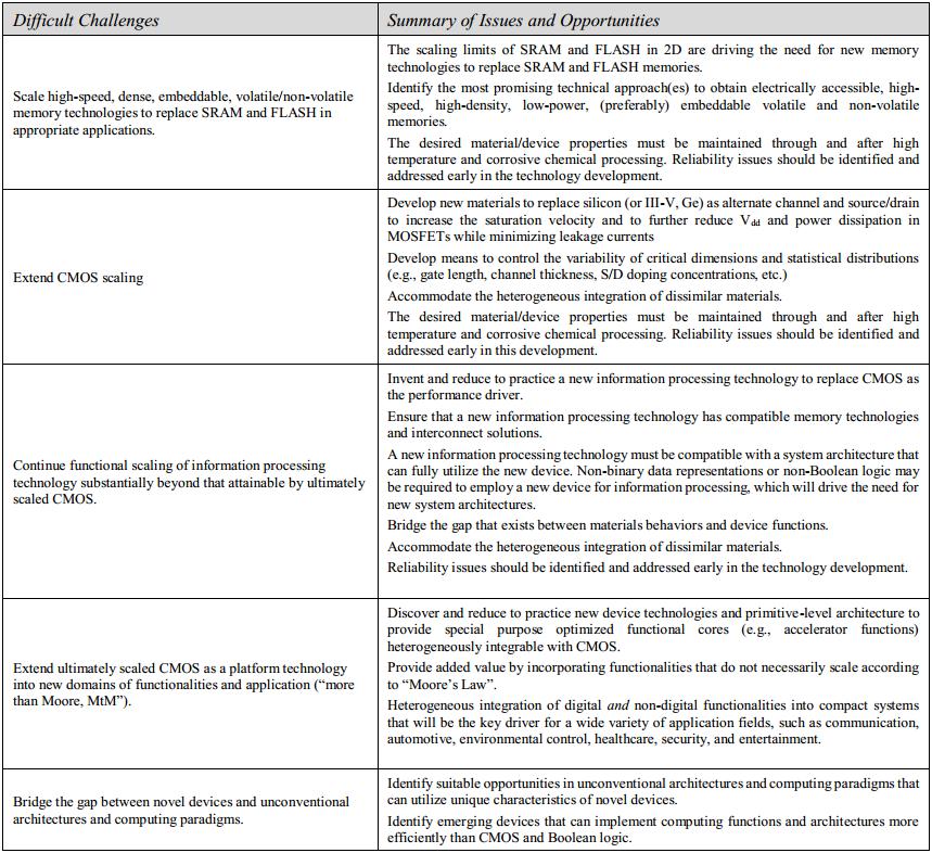 1) What is the possible meaning of the a.k.a. in the first paragraph? ( ) A all kill all B also known as C as known as D as known about 2) Which of the following is not the disadvantage of the current evolutionary solution? ( ) A accessible non-volatile memory B a decrease of the net information throughput C requirement of external storage media with slow access D increasing the floor space that SRAM occupies on an MPU chip 3) According to this article, we need a new memory technology to ( ) A combine the best features of current memories in a fabrication technology compatible with CMOS process flow and that can be scaled beyond the present limits of SRAM and FLASH. B provide a memory device fabrication technology required for both stand-alone and embedded memory applications. C provide a significant increase in information throughput. D all of the above 4) Which of the following is not the difficult challenge for a new material device? ( ) A heterogeneous fabrication of high-quality (i.e., defect free) channel and source/drain materials on non-lattice matched silicon. B minimization of band-to-band tunneling in narrow bandgap channel materials. C to sustain the required leakage currents through the high-κ gate dielectrics on the passivated channel materials. D elimination of Fermi level pinning in the channel/gate dielectric interface. 5) According to this article, emerging research device may not be ( ) A compatible with Boolean logic B manufacturable C for special purpose D with high efficiency 6)Functional diversification is a way to add value to devices by ( ) . A incorporating functionalities. B High-k gate. C Moore’s Law. D new channel material. 7)The author implies that it is possible ( ) while introduce the new materials into the MOSFET. A to develop a non-binary data representation B to provide a significant increase in information throughput beyond the traditional benefits of scaling C to be a challenge to control the variations in critical dimensions and statistical fluctuations D to improve the ability of an MPU to execute programs 8) According to the article, which of the following description of the next generation information processing technology is false?( ) A Emerging research devices might be used to realize special purpose processor cores that could be integrated with multiple CMOS CPU cores. B The emerging research device technology may eventually replace the CMOS gate as a new information processing primitive element. C A non-binary data representation and non-Boolean logic may be required to employ a new device for information processing. D emerging research device is required for information processing without a system architecture. 9) Reliability issues should be identified and addressed early in the development of ( ) A new memory technologies to replace SRAM and FLASH. B new device technologies to extend CMOS scaling. C Continue functional scaling of information processing technology. D all of the above. 10) Which of the following we may not achieve from the new channel material MOSFETs ? ( ) A the increase of the saturation velocity B further reduction of Vdd and power dissipation C non-binary data representations D minimization of leakage currents
 题目内容
(请给出正确答案)
题目内容
(请给出正确答案)
 简答题官方参考答案
(由简答题聘请的专业题库老师提供的解答)
简答题官方参考答案
(由简答题聘请的专业题库老师提供的解答)
 抱歉!暂无答案,正在努力更新中……