听力原文:M: Hello.W: Hello, Sam...this is Paula Hansen. Sorry to bother you, but I'm havin
听力原文:M: Hello.
W: Hello, Sam...this is Paula Hansen. Sorry to bother you, but I'm having a small problem I thought you might be able to help me with.
M: Sure, Paola. What's up?
W: Well, you know Sarah and I moved into an off-campus apartment in the fall...over on the west side of town. Anyway, we've been happy with it until the past couple of months.
M: Yeah? What happened?
W: Well, the dishwasher broke down, se we reported it to Ms. Connors, the owner. She said she'd take care of it, but a month went by and nothing happened.
M: Did you get back in touch with her?
W: I got a repair person to give me an estimate. Then I sent it to her. When I didn't hear from her, I had the repair done. And I deducted the cost from the rent check.
M: So what's the problem?
W: She called here mad as a hornet. She said she could've gotten the repair done for less money. Now she's threatening to evict us for not paying the full rent.
M: Hold on, Panic. It does sound pretty serious, but I'm sure you can all sit down and work this out.
W: Well, you're over at the law school, so I wondered if you would mind coming with Sarah and me when we go to talk to Ms. Connors. We're supposed to meet with her tomorrow night at 8:00.
(20)
A.The apartment is too far from the campus.
B.The apartment needs a lot of repair work.
C.She's having trouble with the owner of the apartment.
D.Her roommate won't share expenses.
 题目内容
(请给出正确答案)
题目内容
(请给出正确答案)
 简答题官方参考答案
(由简答题聘请的专业题库老师提供的解答)
简答题官方参考答案
(由简答题聘请的专业题库老师提供的解答)
 抱歉!暂无答案,正在努力更新中……

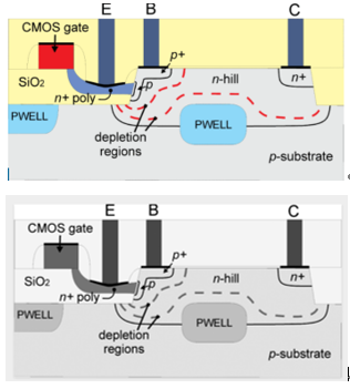 Cross section of the (1) is shown in Fig. 1. The structure is similar to the reported single polysilicon region HCBT [9]. The only difference is that the CMOS p-well region is implanted (2) the certain distance (3) the intrinsic base (4) the collector n -hill region. Standard HCBT process is described in [8] and [9]. Transistors are fabricated in the silicon islands defined by the shallow trench isolation process using a CMOS activemask. HCBT collector marked as (5) in Fig. 1 is implanted using an n-hill mask with the same implantation parameters as in [10]. An oxide etching mask is used for the formation of an emitter trench and it defines the (6) of the emitter (lE) , which extends out of the plane in the cross section of Fig. 1. The CMOS p-well implant is also used for the isolation of HCBT devices (7) a channel stopper shown in Fig. 1. Base and n+ collector masks are used for the intrinsic/extrinsic bases and the n+ collector implantations, respectively. The CMOS (8) next to the emitter trench (Fig. 1) is electrically inactive and is used to improve reliability of the emitter polysilicon processing [9].