题目内容
(请给出正确答案)
题目内容
(请给出正确答案)
提问人:网友chenjia876
发布时间:2022-01-06
[单选题]
关于借贷记账法试算平衡的表述中,不正确的是().
A.试算平衡的根据是资产与权益的恒等关系和借贷记账法的记账规则
B.试算平衡的方法包括发生额试算平衡法和余额试算平衡法
C.试算平衡表借贷不相等,说明账户记录有错误
D.试算平衡表是平衡的,说明账户记录正确
 参考答案
题目内容
(请给出正确答案)
参考答案
题目内容
(请给出正确答案)
A.试算平衡的根据是资产与权益的恒等关系和借贷记账法的记账规则
B.试算平衡的方法包括发生额试算平衡法和余额试算平衡法
C.试算平衡表借贷不相等,说明账户记录有错误
D.试算平衡表是平衡的,说明账户记录正确
参考答案
 更多“关于借贷记账法试算平衡的表述中,不正确的是().A.试算平衡的根据是资产与权益的恒等关系和借”相关的问题
完形填空 Bipolar transistors which have a fully depleted intrinsic collector can be used as high-voltage (HV) devices since they have increased values of breakdown voltages [1]–[2][3][4][5][6][7]. Furthermore, a base width modulation in such structures is suppressed allowing for aggressive scaling of the base layer, which results in a great tradeoff between common-emitter current gain (β) and early voltage (VA) , offering a good analog performance. A high-frequency performance is degraded, but devices working at the Jonhson’s limit are demonstrated [6]. The integration of a horizontal current bipolar transistor (HCBT) with standard 0.18-μmCMOS has been reported in [8] and [9]. A HV double-emitter (DE) HCBT is added to the process at zero additional costs [6]. In the DE HCBT, the intrinsic collector is fully depleted in the normal operation mode and transistors with BVCEO = 12.6 V, are demonstrated. Full depletion of the collector region is obtained by geometrical confinement of the intrinsic collector space charge by using the DE geometry. Recently, a DE HCBT with the reduced-surface-field (RESURF) region was reported with the BVCEOas high as 36 V [7]. It uses the CMOS p-well implant for the formation of local substrate which creates the additional RESURF drift region and improves the BVCEO. In the HCBT BiCMOS technology, a structure with the fully depleted collector can be obtained with single-emitter (SE) geometry as well. This can be accomplished by placing the CMOS p-well region under the n -collector near the intrinsic transistor. When the transistor operates in the normal operation mode, the intrinsic collector charge is shared and the collector is fully depleted. This paper presents a novel HV SE HCBT, which is integrated with the HCBT BiCMOS without additional cost. The structure achieves BVCEO= 10.5 V and fT=15.8 GHz. The electrical performance is comparable to the DE HCBT with medium BVCEO suitable for power amplifier applications. The main advantage over the DE HCBT is the scalability of the emitter length, which offers more flexibility in the physical design of circuits and better area efficiency. All three HV HCBT structures as well as high-speed (HS) HCBT are integrated in the same process flow which uses the steep collector profile reported in [10].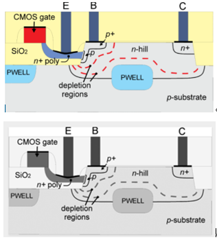 Cross section of the (1) is shown in Fig. 1. The structure is similar to the reported single polysilicon region HCBT [9]. The only difference is that the CMOS p-well region is implanted (2) the certain distance (3) the intrinsic base (4) the collector n -hill region. Standard HCBT process is described in [8] and [9]. Transistors are fabricated in the silicon islands defined by the shallow trench isolation process using a CMOS activemask. HCBT collector marked as (5) in Fig. 1 is implanted using an n-hill mask with the same implantation parameters as in [10]. An oxide etching mask is used for the formation of an emitter trench and it defines the (6) of the emitter (lE) , which extends out of the plane in the cross section of Fig. 1. The CMOS p-well implant is also used for the isolation of HCBT devices (7) a channel stopper shown in Fig. 1. Base and n+ collector masks are used for the intrinsic/extrinsic bases and the n+ collector implantations, respectively. The CMOS (8) next to the emitter trench (Fig. 1) is electrically inactive and is used to improve reliability of the emitter polysilicon processing [9].
(温馨提示:如果图片无法看清,右击在新的标签页打开即可) Dimensional and functional scaling of CMOS is driving information processing technology into a broadening spectrum of new applications. Scaling has enabled many of these applications through increased performance and complexity. As dimensional 1 of CMOS will eventually approach fundamental 2 , several new information 3 devices and microarchitectures for both existing and new functions are being explored to extend the historical integrated circuit scaling cadence. This is driving interest in new devices for information processing and memory, new technologies for heterogeneous integration of multiple functions, and new paradigms for system architecture. The semiconductor industry is facing some difficult challenges related to extending integrated circuit technology to new applications and to beyond the end of CMOS dimensional scaling. One class relates to propelling CMOS beyond its ultimate density and functionality by integrating a new high-speed, high-density, and 4 memory technology onto the CMOS platform. Another class is to extend CMOS scaling with alternative channel 5 . The third class is information processing technologies substantially beyond those attainable by 6 using an innovative combination of new devices, interconnect, and architectural approaches for extending CMOS and eventually inventing a new information processing platform technology. The fourth class is to extend ultimately scaled CMOS as a platform technology into new domains of functionalities and application, also known as “ 7 ”. The fifth class is to bridge the gap between novel devices and unconventional 8 and computing paradigms. These difficult challenges are summarized in Table 1. Table 1
1. Reading Comprehension(每小题2分,共60分) (1) Device Technology Challenges Difficult challenges gating development of beyond-CMOS devices include those related to memory technologies, information processing or logic devices, and heterogeneous integration of multi-functional components, a.k.a. More-than-Moore (MtM) or Functional Diversification. One challenge is the need of a new memory technology that combines the best features of current memories in a fabrication technology compatible with CMOS process flow and that can be scaled beyond the present limits of SRAM and FLASH. This would provide a memory device fabrication technology required for both stand-alone and embedded memory applications. The ability of an MPU to execute programs is limited by interaction between the processor and the memory, and scaling does not automatically solve this problem. The current evolutionary solution is to increase MPU cache memory, thereby increasing the floor space that SRAM occupies on an MPU chip. This trend eventually leads to a decrease of the net information throughput. In addition to auxiliary circuitry to maintain stored data, volatility of semiconductor memory requires external storage media with slow access (e.g., magnetic hard drives, optical CD, etc.). Therefore, development of electrically accessible non-volatile memory with high speed and high density would initiate a revolution in computer architecture. This development would provide a significant increase in information throughput beyond the traditional benefits of scaling when fully realized for nanoscale CMOS devices. A related challenge is to sustain scaling of CMOS logic technology. One approach to continuing performance gains as CMOS scaling matures in the next decade is to replace the strained silicon MOSFET channel (and the source/drain) with an alternate material offering a higher potential quasi-ballistic-carrier velocity and higher mobility than strained silicon. Candidate materials include strained Ge, SiGe, a variety of III-V compound semiconductors, and carbon materials. Introduction of non-silicon materials into the channel and source/drain regions of an otherwise silicon MOSFET (i.e., onto a silicon substrate) is fraught with several very difficult challenges. These challenges include heterogeneous fabrication of high-quality (i.e., defect free) channel and source/drain materials on non-lattice matched silicon, minimization of band-to-band tunneling in narrow bandgap channel materials, elimination of Fermi level pinning in the channel/gate dielectric interface, and fabrication of high-κ gate dielectrics on the passivated channel materials. Additional challenges are to sustain the required reduction in leakage currents and power dissipation in these ultimately scaled CMOS gates and to introduce these new materials into the MOSFET while simultaneously minimizing the increasing variations in critical dimensions and statistical fluctuations in the channel (source/drain) doping concentrations. The industry is now addressing the increasing importance of a new trend of functional diversification, where added value to devices is provided by incorporating functionalities that do not necessarily scale according to “Moore's Law”. A longer-term challenge is invention and reduction to practice of a manufacturable information processing technology addressing “beyond CMOS” applications. For example, emerging research devices might be used to realize special purpose processor cores that could be integrated with multiple CMOS CPU cores to obtain performance advantages. These new special purpose cores may provide a particular system function much more efficiently than a digital CMOS block, or they may offer a uniquely new function not available in a CMOS-based approach. Solutions to this challenge beyond the end of CMOS scaling may also lead to new opportunities for such an emerging research device technology to eventually replace the CMOS gate as a new information processing primitive element. A new information processing technology must also be compatible with a system architecture that can fully utilize the new device. A non-binary data representation and non-Boolean logic may be required to employ a new device for information processing. These requirements will drive the need for new system architectures. The requirements and opportunities correlating emerging devices and architectures are discussed in the “Emerging Device-Architecture Interaction” section. Table 1 Beyond CMOS Difficult Challenges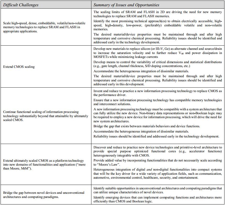 1) What is the possible meaning of the a.k.a. in the first paragraph? ( ) A all kill all B also known as C as known as D as known about 2) Which of the following is not the disadvantage of the current evolutionary solution? ( ) A accessible non-volatile memory B a decrease of the net information throughput C requirement of external storage media with slow access D increasing the floor space that SRAM occupies on an MPU chip 3) According to this article, we need a new memory technology to ( ) A combine the best features of current memories in a fabrication technology compatible with CMOS process flow and that can be scaled beyond the present limits of SRAM and FLASH. B provide a memory device fabrication technology required for both stand-alone and embedded memory applications. C provide a significant increase in information throughput. D all of the above 4) Which of the following is not the difficult challenge for a new material device? ( ) A heterogeneous fabrication of high-quality (i.e., defect free) channel and source/drain materials on non-lattice matched silicon. B minimization of band-to-band tunneling in narrow bandgap channel materials. C to sustain the required leakage currents through the high-κ gate dielectrics on the passivated channel materials. D elimination of Fermi level pinning in the channel/gate dielectric interface. 5) According to this article, emerging research device may not be ( ) A compatible with Boolean logic B manufacturable C for special purpose D with high efficiency 6)Functional diversification is a way to add value to devices by ( ) . A incorporating functionalities. B High-k gate. C Moore’s Law. D new channel material. 7)The author implies that it is possible ( ) while introduce the new materials into the MOSFET. A to develop a non-binary data representation B to provide a significant increase in information throughput beyond the traditional benefits of scaling C to be a challenge to control the variations in critical dimensions and statistical fluctuations D to improve the ability of an MPU to execute programs 8) According to the article, which of the following description of the next generation information processing technology is false?( ) A Emerging research devices might be used to realize special purpose processor cores that could be integrated with multiple CMOS CPU cores. B The emerging research device technology may eventually replace the CMOS gate as a new information processing primitive element. C A non-binary data representation and non-Boolean logic may be required to employ a new device for information processing. D emerging research device is required for information processing without a system architecture. 9) Reliability issues should be identified and addressed early in the development of ( ) A new memory technologies to replace SRAM and FLASH. B new device technologies to extend CMOS scaling. C Continue functional scaling of information processing technology. D all of the above. 10) Which of the following we may not achieve from the new channel material MOSFETs ? ( ) A the increase of the saturation velocity B further reduction of Vdd and power dissipation C non-binary data representations D minimization of leakage currents
(2) 3D Heterogeneous Integration Every logic generation needs to add new functions in each node to keep unit price constant (to preserve margins). This is getting more difficult due to the following challenges: • Little functions left on board/system to co-integrate • Heterogeneous cores specialized per function—specialized performance improvement requirements needed per each dedicated core • Off-package memories—costly to co-integrate with logic, technology not fitting to baseline CMOS (where wafer/die-level stacking might be needed) Die cost reduction has been enabled so far by concurrent scaling of poly pitch, metal pitch, and cell height scaling. This would like to continue until 2024. Cell height scaling would likely to be pursued by 3D device (e.g., finFET and lateral GAA), device stacking, 3DVLSI, and design-technology-co-optimization (DTCO) constructs in cell and physical design. However, this scaling route will become challenged by diminishing electrical/system benefits and also by diminishing areareduction/$ at SoC level. Therefore, it is necessary to pursue 3D integration routes such as device-over-device stacking and/or monolithic 3D (or sequential integration) These pursuits will maintain system performance and power gains while maintaining the cost advantages such as treating expensive non-scaled components somewhere else and using the best technology fit per tier functionality. 3DVLSI offers the possibility to stack devices enabling high-density contacts at the device level (up to 100 million vias per mm² with N14 ground rules). 3DVLSI can be routed either at gate or transistor levels. The partitioning at the gate level allows IC performance gain due to wire length reduction while partitioning at the transistor level by stacking nFET over pFET (or the opposite), enabling the independent optimization of both types of transistors (customized implementation of channel material/substrate orientation/channel and raised source/drain strain, etc.) while enabling reduced process complexity compared to a planar co-integration, for instance the stacking of III-V nFETs above SiGe pFETs. These high mobility transistors are well suited for 3DVLSI because their process temperatures are intrinsically low. 3DVLSI, with its high contact density, can also enable applications requiring heterogeneous co-integration with high-density 3D vias, such as NEMS with CMOS for gas sensing or highly miniaturized imagers. In order to address the transition from 2D to 3DVLSI, the following generations are projected in the IRDS roadmap: • Die-to-wafer and wafer-to-wafer stacking o Approach: Fine-pitch di-electric/hybrid bonding and/or flip-chip assembly o Opportunities: Reducing bill-of-materials on the system, heterogenous integration o Challenges: Design/architecture partitioning • N&P stacking o Approach: Sequential integration o Opportunities: Reducing 2D footprint of standard cell o Challenges: Minimizing interconnect overhead is key between N&P enabling low-cost • Adding logic 3D SRAM and/or MRAM stack (embedded/stacked) o Approach: Sequential integration and/or wafer transfer o Opportunities: 2D area gain, better connection between logic and memory enabling system latency gains. o Challenges: Solving the thermal budget of interconnect at the lower tier if stacking approach is used, Revisiting the cache hierarchy and application requirements, power, and clock distribution • Adding Analog and I/O o Approach: Sequential integration and/or wafer transfer o Opportunities: Giving more freedom to designer and allows integration of high-mobility channels, pushing non-scaling components to another tier, IP re-use, scalability, IO voltage enablement in advanced nodes o Challenges: Thermal budget, reliability requirements, power and clock distribution • True-3D VLSI: Clustered functional stacks, beyond CMOS adoption o Approach: Sequential integration and/or wafer transfer o Opportunities: Complementary functions other than CMOS replacement such as neuromorphic, highbandwidth memory. Application examples include image recognition in neuromorphic fabric and wideIO sensor interfacing (e.g., DNA sequencing, molecular analysis). o Challenges: Architecting the application where low energy at low frequency and highly-parallel interfaces could be utilized, mapping applications to non-Von Neumann architectures. 1) Which of the following may not be the challenge to add new functions in each node of logic generation? ( ) A Little functions left on board/system to co-integrate B Heterogeneous cores specialized per function—specialized performance improvement requirements needed per each dedicated core C Technology not fitting to baseline CMOS D SRAM and FLASH memories 2) Which of the following may not reduce the die cost? ( ) A Scaling of pecialized performance B Scaling of poly pitch C Scaling of metal pitch D Scaling cell height 3) Cell height scaling would likely to be pursued by ( ) A 3D device B Device stacking C 3DVLSI D all of the above 4) 3D integration routes may not include ( ) A device-over-device stacking B scaling of poly pitch C sequential integration D monolithic 3D 5) We can maintain the cost advantages by ( ) for 3D integration. A using new materials for channel B using high κ dielectrics for gate C treating expensive non-scaled components somewhere else D Moore’s Law 6) According to the author, which of the following is false? ( ) A 3DVLSI may achieve high-density contacts at the device level. B 3DVLSI can be routed either at gate or transistor levels. C 3DVLSI allows IC performance gain due to wire length reduction D 3DVLSI may enable the optimization of one type of transistors. 7) What is the challenge for monolithic 3D integration? ( ) A Design of the system B Architecture C Minimizing interconnect overhead D Applications requiring heterogeneous co-integration with high-density 3D vias 8) What is the advantage of the N&P stacking? A Reducing bill-of-materials on the system B Reducing 2D footprint of standard cell C Reducing the thermal budget of interconnect D All of the above 9) According to the author, which of the following can achieve the 2D area gain? ( ) A Logic 3D SRAM and/or MRAM stack B Scaling of poly pitch C Scaling of metal pitch D All of the above 10) The author implies that neuromorphic may ( ) A be realized by wafer transfer. B be realized by CMOS solution. C be used in Von Neumann architectures. D be a highbandwidth memory.
2. Fill in the blanks with the appropriate words(每小题2分,共40分) (1) A 1) is characterized by having a well-structured periodic placement of atoms. The smallest assembly of atoms that can be repeated to form the entire crystal is called a 2) , with a dimension of 3) . (2) For any semiconductor there is a forbidden energy range in which allowed states cannot exist. Energy regions or energy bands are permitted above and below this energy gap. The upper bands are called the 4) ; the lower bands, the 5) . The separation between the energy of the lowest conduction band and that of the highest valence band is called the 6) or energy gap Eg, which is one of the most-important parameters in semiconductor physics. (3) For an n-type silicon, a substitutional phosphorous atom with five valence electrons has replaced a silicon atom and a negative-charged electron is donated to the lattice in the conduction band. The phosphorous atom is called a 7) . When a boron atom with three valence electrons substitutes for a silicon atom, a positive-charged hole is created in the valence band and an additional electron will be accepted to form four covalent bonds around the boron. This is p-type, and the boron is an 8) . We can calculate the approximate distance of the donor electron from the donor impurity ion, and also the approximate energy required to elevate the donor electron into the conduction band. This energy is referred to as the 9) . (4) Electronic devices rely on transport of electrons (holes) in materials. This transport occurs either under the influence of an electric 10) or carrier concentration 11) . There are two collision or scattering mechanisms that dominate in a semiconductor and affect the carrier 12) : phonon or 13) scattering, and 14) scattering. If the carrier energy is large enough it can transfer energy to the lattice by the emission of an optical phonon. This mechanism is very efficient and limits the maximum drift velocity. The limiting value for the drift velocity is termed the 15) . Besides the 16) , which flows when an electric field is applied and which follows Ohm's law, an additional important component of current can flow if a spatial variation of carrier energies or densities exists within the material. This component of current is called 17) . (5) The bipolar transistor has three separately doped regions and two pn 18) . The three terminal connections are called the emitter, base, and 19) . The width of the 20) region is small compared to the minority carrier diffusion length.
A、60万元,60万元
B、60万元,10万元
C、0万元,10万元
D、0万元,60万元


 警告:系统检测到您的账号存在安全风险
为了保护您的账号安全,请在“简答题”公众号进行验证,点击“官网服务”-“账号验证”后输入验证码“”完成验证,验证成功后方可继续查看答案!