完形填空 Bipolar transistors which have a fully depleted intrinsic collector can be used as high-voltage (HV) devices since they have increased values of breakdown voltages [1]–[2][3][4][5][6][7]. Furthermore, a base width modulation in such structures is suppressed allowing for aggressive scaling of the base layer, which results in a great tradeoff between common-emitter current gain (β) and early voltage (VA) , offering a good analog performance. A high-frequency performance is degraded, but devices working at the Jonhson’s limit are demonstrated [6]. The integration of a horizontal current bipolar transistor (HCBT) with standard 0.18-μmCMOS has been reported in [8] and [9]. A HV double-emitter (DE) HCBT is added to the process at zero additional costs [6]. In the DE HCBT, the intrinsic collector is fully depleted in the normal operation mode and transistors with BVCEO = 12.6 V, are demonstrated. Full depletion of the collector region is obtained by geometrical confinement of the intrinsic collector space charge by using the DE geometry. Recently, a DE HCBT with the reduced-surface-field (RESURF) region was reported with the BVCEOas high as 36 V [7]. It uses the CMOS p-well implant for the formation of local substrate which creates the additional RESURF drift region and improves the BVCEO. In the HCBT BiCMOS technology, a structure with the fully depleted collector can be obtained with single-emitter (SE) geometry as well. This can be accomplished by placing the CMOS p-well region under the n -collector near the intrinsic transistor. When the transistor operates in the normal operation mode, the intrinsic collector charge is shared and the collector is fully depleted. This paper presents a novel HV SE HCBT, which is integrated with the HCBT BiCMOS without additional cost. The structure achieves BVCEO= 10.5 V and fT=15.8 GHz. The electrical performance is comparable to the DE HCBT with medium BVCEO suitable for power amplifier applications. The main advantage over the DE HCBT is the scalability of the emitter length, which offers more flexibility in the physical design of circuits and better area efficiency. All three HV HCBT structures as well as high-speed (HS) HCBT are integrated in the same process flow which uses the steep collector profile reported in [10].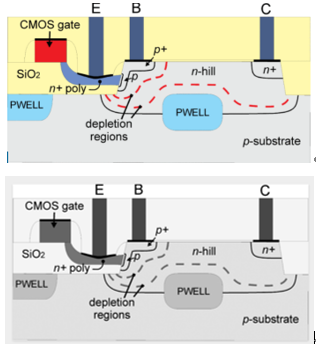 Cross section of the (1) is shown in Fig. 1. The structure is similar to the reported single polysilicon region HCBT [9]. The only difference is that the CMOS p-well region is implanted (2) the certain distance (3) the intrinsic base (4) the collector n -hill region. Standard HCBT process is described in [8] and [9]. Transistors are fabricated in the silicon islands defined by the shallow trench isolation process using a CMOS activemask. HCBT collector marked as (5) in Fig. 1 is implanted using an n-hill mask with the same implantation parameters as in [10]. An oxide etching mask is used for the formation of an emitter trench and it defines the (6) of the emitter (lE) , which extends out of the plane in the cross section of Fig. 1. The CMOS p-well implant is also used for the isolation of HCBT devices (7) a channel stopper shown in Fig. 1. Base and n+ collector masks are used for the intrinsic/extrinsic bases and the n+ collector implantations, respectively. The CMOS (8) next to the emitter trench (Fig. 1) is electrically inactive and is used to improve reliability of the emitter polysilicon processing [9].
 题目内容
(请给出正确答案)
题目内容
(请给出正确答案)
 参考答案
参考答案
 简答题官方参考答案
(由简答题聘请的专业题库老师提供的解答)
简答题官方参考答案
(由简答题聘请的专业题库老师提供的解答)
 网友提供的答案