题目内容
(请给出正确答案)
题目内容
(请给出正确答案)
提问人:网友qq283876581
发布时间:2022-01-06
[主观题]
This article, the second in a series, goes into more __________ technical detail.
 简答题官方参考答案
(由简答题聘请的专业题库老师提供的解答)
简答题官方参考答案
(由简答题聘请的专业题库老师提供的解答)
 抱歉!暂无答案,正在努力更新中……
题目内容
(请给出正确答案)
简答题官方参考答案
(由简答题聘请的专业题库老师提供的解答)
抱歉!暂无答案,正在努力更新中……
抱歉!暂无答案,正在努力更新中……
题目内容
(请给出正确答案)
简答题官方参考答案
(由简答题聘请的专业题库老师提供的解答)
抱歉!暂无答案,正在努力更新中……
 更多“This article, the second in a series, goes into more __________ technical detail.”相关的问题
In order to understand and to evaluate evaporated thin films of CdS for their use in electronic devices, a number of diode structures have been extensively studied. These diodes were made rectifying by exploiting the differing properties of metal contacts to the CdS. The metals used behaved as predicted by the classical Schottky theory. Experiments performed under forward bias established that space-charge-limited currents were flowing in the CdS films. These currents indicated a mobility roughly ⅓ to ½ that of single crystal material. Under reverse-bias conditions, Schottky high-field emission was observed. To verify the existence of space-charge-limited currents under forward-bias conditions, the theoretically-predicted inverse-cube dependence for the current as a function of electrode spacing was measured. The square-law currents in the space-charge-limited region implied a free-to-trapped charge ratio of the order of 10 -2 . The position of the Fermi level in the material indicated, however, that this relatively high free-to-trapped-charge-ratio stemmed from compensation of the deep trapping centers. Free-electron mobilities for the films of up to 100 cm 2 /volt sec was measured by observing space-charge-limited currents under pulsed conditions. Values for the mobility were checked by using time-of-flight measurements. These same measurements showed a qualitative agreement with the theory of transient space-charge-limited currents. Under reverse-bias conditions, Schottky-emission observations allowed a calculation of the Richardson factor for the Au-CdS junction that was close to the theoretical value of 120 amps cm -2 deg -2 . Capacitance measurements under reverse bias indicated a true Schottky barrier. These measurements could be used to determine the extent of the penetration of the space-charge region into the CdS film, and thereby to establish the correspondence of the theoretical Schottky-emission field with that measured. 1. The electronic devices studied in this article are () A resistors B capacitors C transistors D diodes 2. The semiconductor studied in this article is () A silicon B germanium C CdS D ZnO 3. The molibities of the carriers in the films are () those in the single crystal material A higher than B lower than C the same as D The above answers are all correct 4. To verify the existence of space-charge-limited currents under forward-bias conditions, () was measured A the theoretically-predicted inverse-cube dependence for the current as a function of electrode spacing B the position of the Fermi level in the material C Free-electron mobilities for the films D Richardson factor for the Au-CdS junction 5. The free-to-trapped charge ratio is () A in the order of 10 -2 B relatively high C stemmed from compensation of the deep trapping centers D The above answers are all correct
A.70 sec
B.140 sec
C.240 sec
D.270 sec
&8226;Read the article below about career planning.
&8226;Choose the best sentence from below the passage to fill each of the blanks.
&8226;For each gap (8-12), mark one letter (A-G) on your Answer Sheet.
&8226;Do not use arty letter more than once.
Advice on Staff Career Development
For many employees, automatic promotion up the ranks of a company is becoming increasingly rare. A new study suggests that, in response, employers need to consider how they can help staff develop their careers.
Employers need to rethink their approach to career management completely, according to the latest research by the Institute of Employment Studies. The new study finds that in fact there is little opportunity for individual career development in many large organizations. The main reasons for this, it concludes, are the recent cuts in the number of middle-management posts, and the changes that have taken place in the responsibilities of personnel departments. The Institute of Employment Studies makes it clear that it is not good practice for companies to hand over career development-to individual employees and then simply leave them to get on with it. (8)
So how should employers help their staff develop a career? Most employees have come to accept that career development is not always the same thing as upward promotion and a higher salary. (9) They must also ensure that these opportunities are extended to all their staff and not just to selected individuals.
Nick Bridges, who is Director of Human Resources Policy at the Bank of Eastern England, believes there is more talk than action in this area. (10) One way, he believes, for companies to show how serious they are about individual learning is lo make it an official part of company practice, as the Bank of Eastern England has done. (11) This document, he points out, has made the role of managers clear, and the company has also invested huge amounts of money educating managers so that they can then train their staff.
Another company, British Chemicals. has contracted an independent organization to help staff with confidential career advice. According to John rates, the head of Individual Learning and Development at British Chemicals. there is an important role for outside agencies to play in the career management process. He adds that it is company policy for managers to give all staff 'roadmaps' which show possible career routes within the company structure. (12) This has worked especially well. he says, for staff who are used to depending on their line managers for guidance.
Many large organizations now recognize that career development cannot be regarded in isolation, and must be part of an overall business strategy. Human Resources has a real role to play in building a strong workforce which meets a company's long-term business needs and makes it more competitive.
A. Its policy statement says that by 2006, eighty percent of its stall' will have a professional qualification.
B. He argues that while Human Resources managers are saying the way forward is through self-managed learning and self-development, they are still failing to provide adequate learning resources.
C. This change of attitude means employers need to place more emphasis on giving staff the chance to develop a range of skills through horizontal job moves.
D. It points out that employees need to know what the overall company's vision is in order to achieve it.
E. The problem that often arises is that, while they are increasingly encouraged to manage their own careers, they arc not provided with the knowledge and training to do this.
F. They are able to sec that, contrary to expectations, jobs in different fields are similar
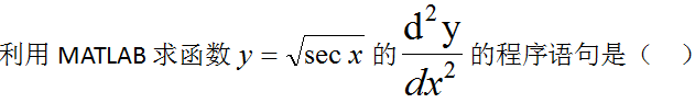
A.syms x; diff(sqrt(sec(x)), 2)
B.syms x; dif(sqrt(sec(x)))
C.syms y; dif(sqrt(sec(x)))
D.syms y; diff(sqrt(sec(x)), 2)


 警告:系统检测到您的账号存在安全风险
为了保护您的账号安全,请在“简答题”公众号进行验证,点击“官网服务”-“账号验证”后输入验证码“”完成验证,验证成功后方可继续查看答案!